Polyphonic pickup, mixed signal
repository: polypu
Although the excruciating uncertainty of not knowing seems like a natural condition of life, this project will inevitably find answers to the questions that keep haunting it, if and when it takes form. In this case, it’s the unknown (im)probability that a mixed-signal assembly might yield the analog performance we’re looking for.
The assembly here would be something that fits into the footprint of a generic humbucking pickup, and one that would send digital audio to a host computer over USB. This project focuses on multiple digital channels, and it’s not obvious where that digitization should happen. Without listing examples, many of the various experimental pickups out there not only avoid putting digital circuitry near the coils, some of them carry the raw signal elsewhere before any amplification.
Even after seeing the worrying measurements of probing the breadboard prototype with an inductor coil, and even knowing of no designs that do so, the possibility of compressing the circuit into the footprint of a common humbucker is tantalizing. The main draw seems to be that keeping the assembly to a single integrated device puts fewer restrictions on what kind of guitar bodies it could be installed into, and it could yield installations that have less mechanical interference with internal and external surfaces.
Schematics
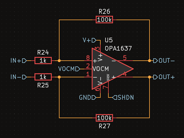
To start in the same place where the road to a finished PCB begins, let’s look at the circuit itself. Each channel consists of a pair of coils wired in parallel and out of phase, feeding into a fully differential amplifier that adds 100 V/V (or 40 dBV) gain, and ends up at the differential input of the ADC, which communicates with the MCU, the only external connection of which is USB FS (full speed).
The amplifier topology is fairly standard for a fully differential amplifier. It’s possible that the feedback resistor values could or should be higher or lower, I’m not sure at this point as I haven’t made the measurements that would help me decide. As for VOCM, although connecting a 100 nF bypass to it could be enough to let the amplifier set its common mode voltage to mid-supply, I wanted to try splitting the MICBIAS output of each ADC with a voltage divider. Not pictured here is a 100 nF bypass capacitor.
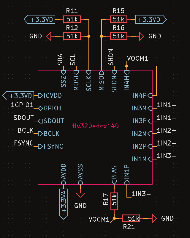
While breadboarding, I have controlled the ADC over SPI, as it was easier for me to set that up initially. However, daisy-chaining multiple TLV320ADC3140s on a single bus requires control over I2C. As far as the schematic is concerned, that means fewer wires, but also one pull-up resistor for each. The specification gives the maximum values for these as a function of the bus capacitance and the speed class used. Here, I went with 5.1k resistors, as I already used that value to pull the CC1 and CC2 pins of USB-C down.
With I2C, the SCLK and MISO pins are used to set the address of each device on the bus. Out of the two 51k resistors on each, only one is meant to be populated; this option makes the addresses easier to adjust later. Initially, I gave them 1 MOhm values, but I was cautioned to make them an order of magnitude lower, as the MOhm range was too close to the input impedances typical of those pins. Internally, the sheet for the ADC adds capacitors in exactly the same topology as the example from the datasheet does.
With I2S, some additional configuration will be required for the ADCs
to be able to share the audio bus. This involves configuring the output
lines and slot assignments in the ASI_CHx registers, as
well as the signaling details in the ASI_CFGx registers.
For instance, the TX_FILL field has to be set if the
outputs are shared, as the ADCs should set their outputs to
high-impedance in bit cycles where they are not transmitting so another
device can drive the output line.
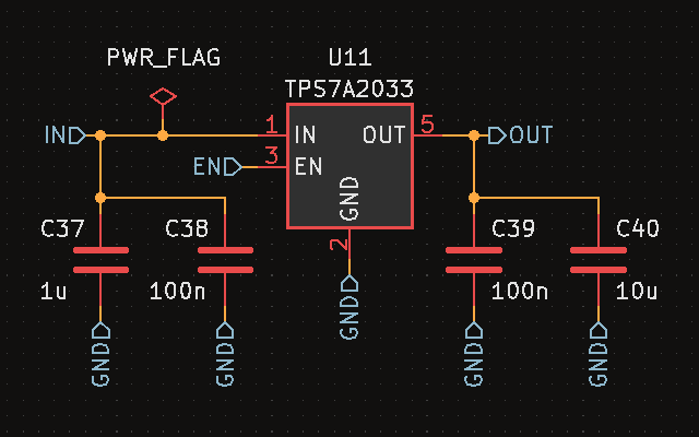
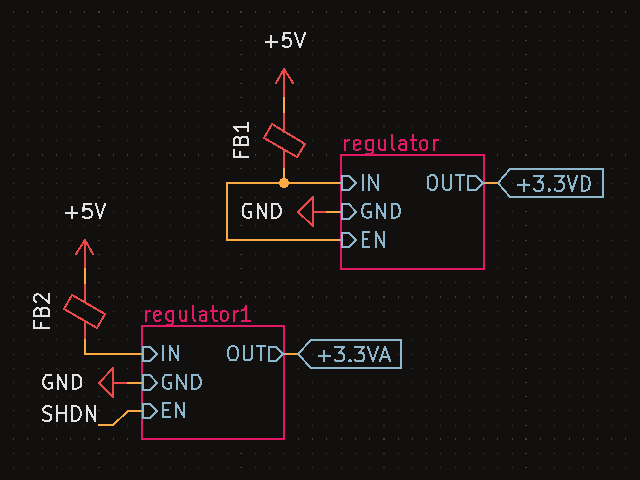
The 5V supply from USB is converted to 3.3V with LDO regulators, one each for the analog and digital circuits. The input/output bypass capacitors here are not gospel, they just seemed okay and I happened to have space for all four of them on the layout.
As an experiment, I followed a suggestion to place a ferrite bead before their inputs, to hopefully attenuate some of the high-frequency noise they emit to or receive from there. Also, don’t be silly like me and note that while the enable pin for the analog one is connected to the shutdown line, the same can’t be done for the digital one, as that will be the one supplying the MCU that will be pulling the shutdown in the first place… thankfully, a keen-eyed colleague caught that (un)happy little accident.
On a related note, don’t forget to double-check the polarities of your shutdown/enable lines. Here, all the above three ICs have either SHDNZ pins (the Z at the end signifying that they are active low, same as a bar over the pin name) or EN pins, meaning that all of them are enabled when the pin goes high and disabled when it goes low.
Speaking of power, let’s see the circuit for the USB connector. As far as the pins are concerned, there are no great surprises here: aside from the classic VBUS/GND/D+/D- pins, only the CC1 and CC2 pins are connected. The two by two connector for the first four pins is an option to let me experiment with soldering directly from a cable to the board. Its connections will be fairly short in the layout, so they shouldn’t affect EMI/EMC measurably.
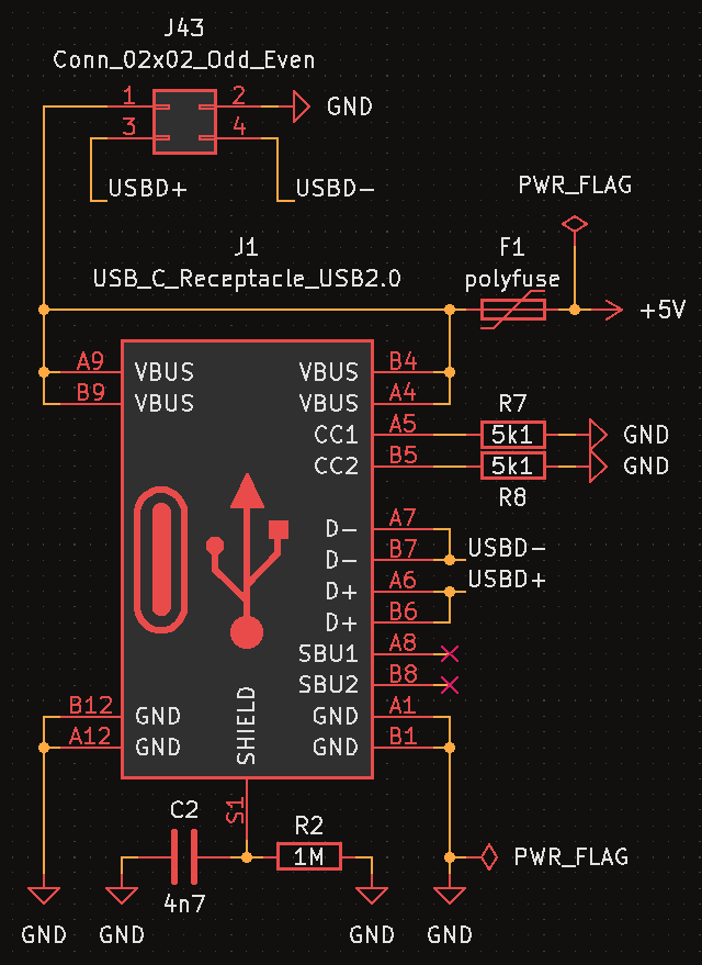
In the analog sense, aside from attach/detach and orientation detection, the CC1/CC2 pins are used for current advertisement. Based on the maximum current the source side can supply, it will pull those lines up to the positive supply with various resistance sizes, which, combined with the pull-down resistors on the sink side, will form a voltage divider. The USB-C specification requires the device port to monitor this voltage corresponding to the current level offered by the host/hub, and to adjust its load dynamically, scaling it back if necessary. Here, the 5.1k resistors serve to hit the voltage range that will indicate the default current level (500 mA for a USB 2.0 port). It’s the lowest level, and still more than this device will need, so I won’t bother monitoring it.
The connector shield is connected to circuit ground through two elements: a resistance and a capacitance. I have added these as options before I have learned that shield and GND are always connected within USB Type-C plugs, so the parallel resistor does almost nothing (since the connection within the plug should be orders of magnitude lower in resistance), and the parallel capacitor will effectively have its terminals shorted together by such a low impedance connection. During later testing, the plug and receptacle shells didn’t always have a solid connection while plugged in, so I ended up desoldering these elements and shorted their pads to connect the receptacle shell to circuit ground.
One element I haven’t used before is known as the polyfuse (also called a “polymeric positive temperature coefficient device” when it’s in trouble). It goes on the VBUS line before all other elements, and should stop excessive current flows after it heats up in a split second, and reduce its resistance back to nominal once it cools down again. It doesn’t seem like a necessary part of devices such as this one, I just wanted to try it out.
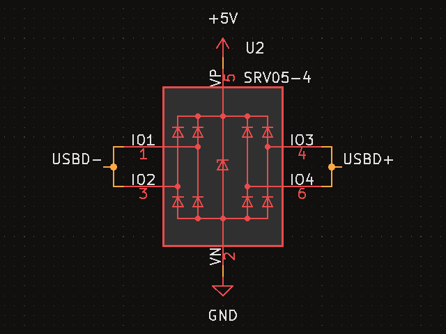
The D+ and D- lines pass by an SRV05-4 transient voltage suppressor (TVS) on their way from the USB connector to the MCU pins.
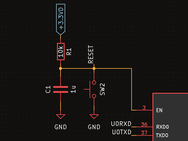
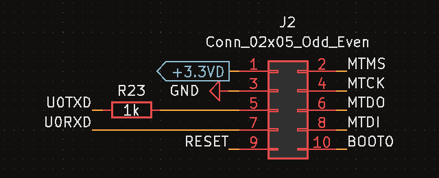
The ESP32 series of chips have an enable pin that can enable the chip when it is high and reset the chip when it is low. Before pulling up this pin, though, the power rails need some time to stabilize (in the case that both start at ground potential), with the minimum specified at 50 us. To ensure the correct timing, the manufacturer recommends adding an RC delay circuit on this pin (a resistance in series and a capacitor to ground, forming a low-pass filter). This delay also ensures that the pin stays below a certain threshold for the same length of time during a reset. The recommended values of 10 kOhm and 1 uF yield a -3dB cutoff frequency of 16 Hz, which sounds like more than enough. To keep things simple, I’ll be pulling this line low manually, with a normally open (NO) button/switch.
Boot parameters for the chip are configured through “strapping pins”, which have latches behind them. At system reset, the latches sample the bit values of their respective pins and store them until the chip is disabled, and they will not change their values in any other way. This makes these values available throughout the chip’s operation, and these pins are free to be used as GPIO pins after reset. The default values of these pins are determined by internal weak (high value) pull-up or pull-down resistors, whenever they have no external connection or a high impedance connection.
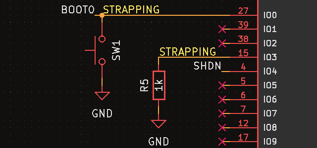
Of these strapping pins, the GPIO0/GPIO46 pair might be the most important, as they control the boot mode. GPIO46 controls the printing of ROM messages in a configurable way, it just has to be low when we wish to enter “joint download boot” mode, to download binary data through UART0 or USB to flash or SRAM. In this case, GPIO0 has to be low. If it is high, GPIO46 can be any value, and in this “SPI boot” mode the ROM bootloader will load and execute the program in SPI flash. As before, I’ll be pulling this line manually. As for GPIO46, it has an internal weak pull-down, so I’ll just leave it unconnected, as I don’t care about enabling or disabling the ROM messages at this point.
The GPIO3 strapping pin is used to control the source of JTAG signals. It has no internal pull resistors, and it must be controlled by an external circuit that cannot be left in a high impedance state. Since I want my JTAG signals to come from the JTAG pins (MTDI/MTCK/MTMS/MTDO), I have to pull the pin low. That, in combination with some EFUSE bits, will help to select those as the source.
The last element adds a bit of utility and convenience, in the form of a 2x5 connector. Aside from the UART RX/TX and JTAG signals, it also has the RESET and BOOT0 nets routed to it, to avoid relying solely on the buttons for resetting and programming.
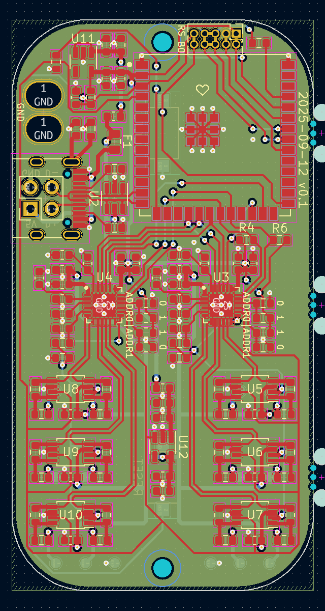
Layout
The boards are designed to fit together as a sandwich, with the ~4-5 mm gap between them bridged electrically through pogo pins. The stackup is a common 4-layer one, with a 1.6 mm total thickness and a 0.2 mm gap between the outer and inner copper layers. To make the most of this proximity, both inner layers are chosen to be reference planes at the same ground potential. The outer layers host a mix of power and signals, with the front layer carrying the most important signals and the back layer carrying most of the sprawling power traces. Assembly is meant to be single-sided to reduce complexity and cost (excluding the tactile buttons and the pickup coils).
In the spirit of separating A/D sections, one half of the processor board is meant to be a digital section, and the other is meant to be an analog one, with the ADCs bridging the two at the center. Most of the passive elements have 0603 footprints, as I wanted to keep this board somewhat reworkable and that is the smallest size I can be bothered to solder by hand. The courtyards are generously large and the resulting density is mercifully small for the same reason.
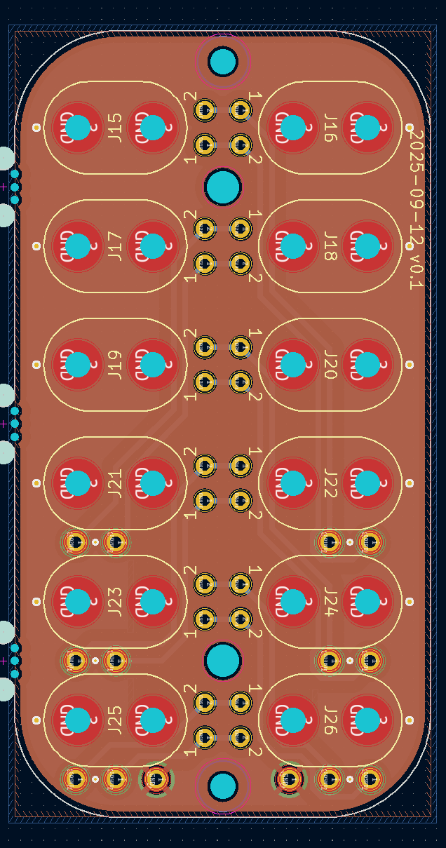
The sensing board is home to the twelve coils acting as six humbuckers, as well as the pogo pins that carry their signals to the processor board. Other than the back layer connecting these, all layers are filled with ground. The holes between the first and second and the fifth and sixth strings allow access to the RESET and BOOT0 buttons.
In hindsight - to the surprise of probably no one - the board could be improved. The hole tolerances were too loose, with 2.2 mm for the two main M2 screws, and 2.14 mm for those that go into the coils. Since then, I’ve learned that using screws for aligning faces horizontally isn’t often done in mechanical design, but it’s kind of hard to get away from in this assembly. For prototyping, I have used 4 mm countersunk screws, which helped with positioning the coils somewhat. The clearance of some components to the board edge could have been larger in a few places, to avoid just barely getting away with 0.8 mm printed walls around them.
Assembly
This double-decker of a sandwich consists of a bottom plate, a spacer in the middle, a cover at the top, and twelve coils. Each coil is printed in two parts, with separate caps that snap onto two pillars in the shape of a waning moon. The following explosion shows a work-in-progress state of just the pickup, omitting the specific mounting frame that I had to model for the guitar it will be installed into. All printed parts were designed with a 0.4 mm nozzle and a 0.2 mm layer height in mind to be printable on cheap FDM printers, and they shouldn’t need supports either.
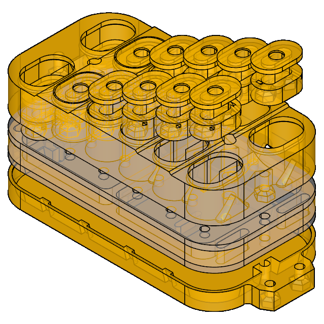
The threading will probably have to change in the future, especially for the two M2 screws holding the bridge together and the four M2 screws it is planned to hang from. The problem with press fitting metric nuts so close to the printed outer perimeters is that a 0.4 mm single wall or even a 0.8 mm double wall can easily flex outwards, and end up too loose even at a tolerance that would make for an acceptable press fit further away from the perimeter. Decreasing the tolerance helps only marginally. I guess I’ll see if they can be replaced with heat set inserts while staying at the same dimensions, since melting such thin walls on some sides could also be a problem.
Still, the most problematic part was the top cover, which was not only tedious to process after printing (to remove the hair-thin strings and other artifacts from its cavities), but it also seemed to believe that it is, in some sense, a banana, and warped appropriately. I haven’t tried printing it with a skirt yet, but I’m not sure if holding it to the build plate harder would help that much. It could also turn out that, due to different stresses in different layers, it ends up naturally assuming the likeness of the noble Musaceae immediately after separating from the plate.
The coil leads are threaded through the plated through holes between each humbucker pair. On the other side, enough solder is added to fill the hole and to form a small dome above it. Then, these blobs are heated with a soldering iron until the insulation on the wire melts, which can be checked by measuring the resistance between them. When soldering the second coil of a humbucker pair, this measurement can serve as a baseline, and its halving indicates that the parallel coil is also connected. It’s a good idea to double-check the polarity before soldering, to make sure the parallel coils are wired out of phase.
Noise floor
Well, after sinking so many resources into fucking around, it would seem the time has come to find out. Let’s check the noise floors of each channel during active transmission to see if this assembly has any chance of being electromagnetically compatible with itself. The following spectra show the first three channels above the digital section. The higher channels above the analog sections were quieter. The pickup was plugged in with a right-angle connector that led the USB cable down and away from it.
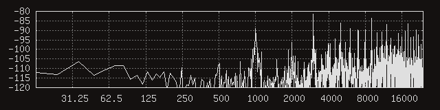
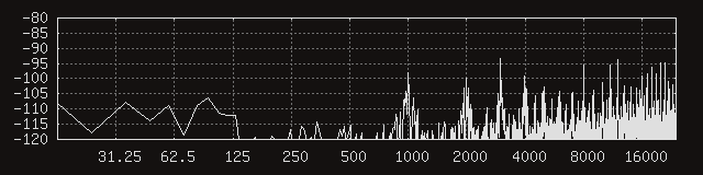
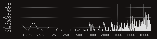
The vertical axis is in dBov, and there’s no doubt that even the individual peaks breach the roughly 96 dB dynamic range of 16 bits, in multiple places. Together, they result in channels that have noise floors well above the quantization noise level.
Before sealing the casket, I should mention that there is still some hope left for this assembly. Through the magic of this post being a month or two behind actual progress, I can tell you that it seems like high-permeability shielding could improve the noise floor considerably. It’s too early to say how far it could push the system forwards, so that will have to be a story for another time.
created
modified