Polyphonic pickup, modules
repository: polypu
The project has been nearing the point beyond which its current means of data acquisition will carry it no further. The low bit depth of the MCP3008, as well as its slow and unsynchronized sampling can no longer carry the weight of our ambitions. After all, it is a general purpose ADC with no specific attributes that would point towards its suitability for high fidelity audio.
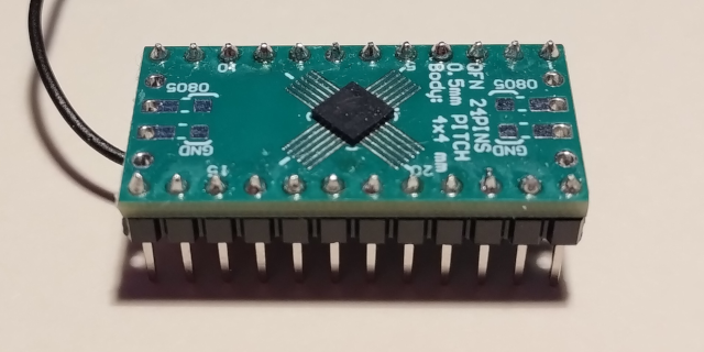
Warping ahead ten years and into the domain of audio ADCs, we arrive at the next candidate: the TLV320ADC3140, a highly integrated converter supporting four analog inputs, 16/20/24/32 bit depths, sample rates reaching 768 kHz, control over SPI/I2C, output over TDM/I2S/LJ, differential as well as single-ended inputs, programmable-gain amplifiers going from 0 dB to 42 dB feeding into a signal processing chain, as well as an abundance of registers which configure all of the above and more. Whew.
However, just as it is written in the Art of Electronics: “woe to the lone basement experimenter-inventor!”, I was met with the miniscule surface-mount packaging of this IC, 24-QFN. With the quarter-millimeter-wide (thin?) leads nearly hidden on the underside, at a pitch of a half millimeter, soldering this package for the first time was a harrowing experience. Not having a board with that footprint to hand at first, I even tried to solder hair-thin copper wires to its leads (fruitlessly). After that, the breakout board I managed to get was so elaborate that it ended up bringing its own set of problems. However, it contacted well enough eventually to let me start figuring out communications.
First light
Thus, it was time to get comfortable with the documentation, in a process that could be best described as staring at the datasheet until morale improves. Thankfully, the datasheet is fairly extensive, and it is accompanied by a host of other documents dealing with more specific topics, such as input coupling and bus sharing.
The example schematic was fairly helpful (aside from the error of
shorting the IOVDD supply to ground), and the only meaningful addition
in my circuit was a 1 MOhm pull-down resistor on the SHDNZ pin.
Initially, I could transition from hardware shutdown to sleep (software
shutdown), following the timed series of events, reading and writing
registers, but I could not get the channels to power up, as the
DEV_STS0 register showed all channels as powered down, and
the bits 7-5 of the DEV_STS1 register were 6d (0b110),
saying that the device is in active mode with all channels turned off.
Turns out I forgot to connect the internal device ground to that of my
own through the thermal pad. After soldering a short wire into a through
hole at the bottom of the breakout board, and connecting it to ground,
the channels could be enabled and the samples could start to flow.
The output on the SDOUT pin looked pretty interesting, too. Starting at the most significant bit, the first 16 or so out of 32 on each channel was a rapidly alternating, continuous 3.3V or GND, fading into noise towards the least significant bit. That’s what a signed representation looks like when a high-pass filter centers the signal around zero! The latter built-in filter is either a programmable first order IIR, or it can just be set to cutoff frequencies of 12 (default), 96, or 384 Hz. Quite convenient, and it saves us a problem to solve.
As a sanity test, I used the stereo output of my phone to verify that the system could capture and stream audio proper. This involved connecting the left and right channels to the single-ended inputs of two inverting amplifier topologies, and connecting the sleeve part of the TRS to a bias voltage generated by a buffer in my circuit. As the fun of listening to this weirdo sound card faded, I realized I should probably figure out what kind of topology would best connect the differential output of some coils to the differential input of the converter. It doesn’t seem like there’s a good reason here to drop down to single-ended in the middle of a differential chain. I wanted to include an amplifier stage in between though, so, at last, it was time to go fully differential.
Modules
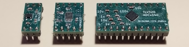
Figuring that it would be some time until I selected some ICs and miscellanea to order, I wanted to try designing a set of breakout modules that would not only adapt the SMD footprints to a 2.54 mm raster, but also connect them in the topologies they would likely end up inhabiting. While I’m still not sure how much of a difference this makes on breadboard or perfboard, this also lets me place the decoupling capacitors and the feedback resistors closer than they could get with a through-hole prototype. They also serve as compact little blocks that can be placed and moved around without much hassle. Lastly, the possibility of using more accurate and less noisy surface-mount resistors is also nice to have.
The first module adds decoupling and filtering capacitors to the converter, and keeps the pinout unchanged.

The second module also adds feedback and gain resistors to a fully differential amplifier, and the third adds two decoupling capacitors to the input and output pins of a low-dropout regulator.
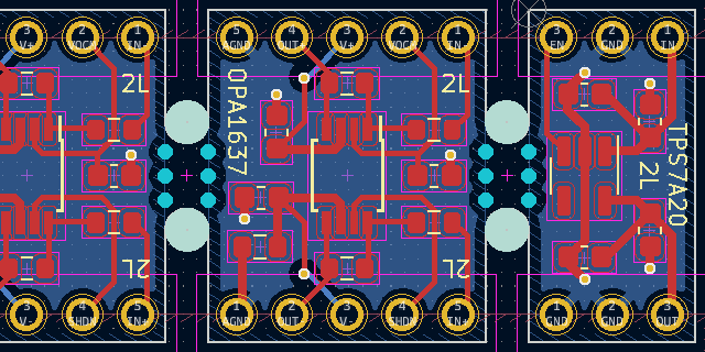
Ten of each of these set of four pieces were manufactured, in both 2-layer and 4-layer variants, where every layer other than the top layer contained a ground pour. The main advantage of a typical 4-layer stackup from a signal integrity and electromagnetic compatibility standpoint comes from the tight spacing between the first two and last two layers, which keeps the fields smaller in volume, and the current loop areas tighter. This only applies to these modules in small ways though, because the grounding of the breadboard or perfboard prototypes they are intended for will not be nearly as good as what can be achieved with a PCB.
System noise
Time to take some early measurements on breadboard and perfboard.
In both cases, the MICBIAS pin of the converter was split with two 50
kOhm resistors to serve as the common-mode voltage input for the VOCM
pin of the amplifier. The input resistors were 1 kOhm, the feedback
resistors were 100 kOhm (both ±0.1%), yielding an amplification of 100
V/V or 40 dB. The converter was configured for line input and DC
coupling in the CHx_CFG0 registers, and all others were
left as default. The regulator supplied both of these, with 100 nF and 1
uF capacitors on both its input and output pins. The noise floor was
measured with the amplifier inputs shorted together. Initially, all
modules were the 2-layer variants.
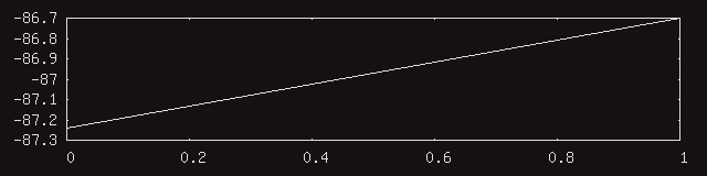
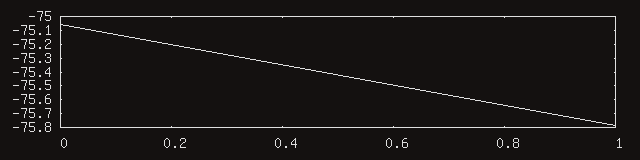
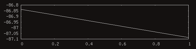
The breadboard circuit measured at -87 dBov, putting it at -127 dBov down from the 2.75 V VREF output of the converter. Swapping all three modules out for 4-layer variants made no measurable difference. Similarly, both variants performed the same on the perfboard prototype as well. It seems that, for this circuit, and for these constructions, the prototyping methods were still not the final limiting factors on noise performance.
Chatter
Having created this measurement instrument of sorts, we can now partake in the sublime joy of pointing it at stuff. Aside from finding the greatest contributors to radiated emissions in the test circuit, it also lets us poke at the question of whether this circuit is even possible to pack into a compact layout without making it flood itself with noise.
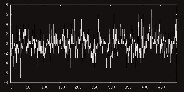
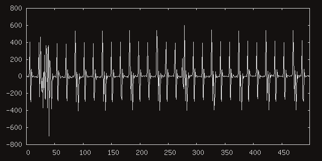
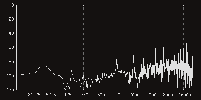
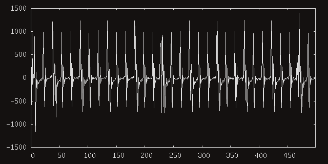
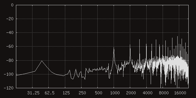
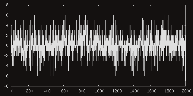
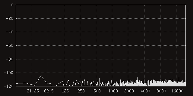
The coil I’ll be pointing at things is a 10 mH, 15 Ohm inductor rated up to 250 mA in a through-hole package with a diameter and height of 11.5 mm. As a zeroeth step, let’s just point it at nothing to start with, up and away from the test circuit sitting at the center of my desk. Different aspects of the same measurement were taken one after the other, so they won’t correlate with each other exactly.
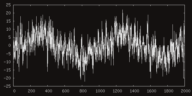
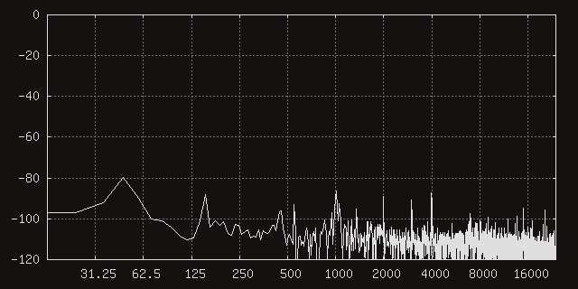
Eyeballing the raw samples could already raise our suspicion about something the spectrum shows clearly: mains hum. The component of this signal with the highest amplitude is the 50 Hz the entire building is humming with. At the very least, this lets us know that the coil is sensitive enough to pick up this common form of interference at a level that can be distinguished from noise.
Next, let’s point the coil against three components on the ESP32-S3-DevKitC.
The MCU module seemed to be the most polite (or the least loud, in any case).
The 5V-to-3.3V LDO had a bit more to say.
The USB-to-UART bridge was the loudest of them all.
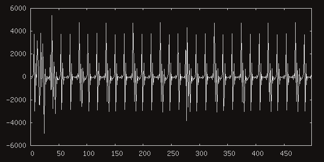

Note that these components might not be responsible for these noise spectra individually. Judging by how similar they look (both in the time and frequency domains), these measurements may all just be showing the same digital switching noise radiating more in some places than others. How exactly this noise is emitted and picked up by my circuit is something I still have no decent mental model for.
Especially with regards to how this relatively low-frequency system could detect the noise coming from digital circuitry that has rising and falling edges orders of magnitude faster than the effective bandwidth of my chain. Both the bandwidth of the coil, the lowered bandwidth of the amplifier due to its high gain, and the anti-aliasing properties of the converter should reject frequencies in those ranges. These peaks could also be subharmonics of higher frequencies, but at this point, I just don’t know enough to explain how they were created.
Humbucking
At last, we find ourselves at the point where we can demonstrate the effectiveness of humbucking at reducing background interference. For this test, I put two of the same through-hole coils (described above) into a breadboard, facing the same way, separated by a few millimeters. They were wired in parallel, and with their polarities reversed (which will result in cancellation, as they were wound in the same direction). Their inductances are specified with a tolerance of ±10%, and these two happened to have a difference in DC resistance of roughly 5%, if that’s indicative of anything.
Magnificent! This humbucking configuration brought us back to the same system noise that we measured with the amplifier inputs shorted together. Even the prominent 50 Hz peak visible in all previous measurements was reduced to below the noise floor and below the 16 bits of precision used in my sample processing code.
A remark I should probably make is that while humbucking does seem to cancel far field interference effectively, it seems less effective at cancelling near field interference (generated by the digital components of this test circuit, for example), especially as the distance to the transmitter decreases and the fields become less uniform. While it does help somewhat, it remains to be seen if self-inflicted fields would permit a compact, mixed-signal design, or the analog and digital sections would need to be split into separate assemblies.
created
modified